Printed Circuit Boards
Consumer electronics

Consumer electronics
Features
Identifying critical defects on Printed Circuit Boards
Our AI provides solutions.
Train a pipeline specific to your defects
Autofocus
Advanced autofocus algorithms determine an autofocus map to deliver precise results across batches.
Benefits
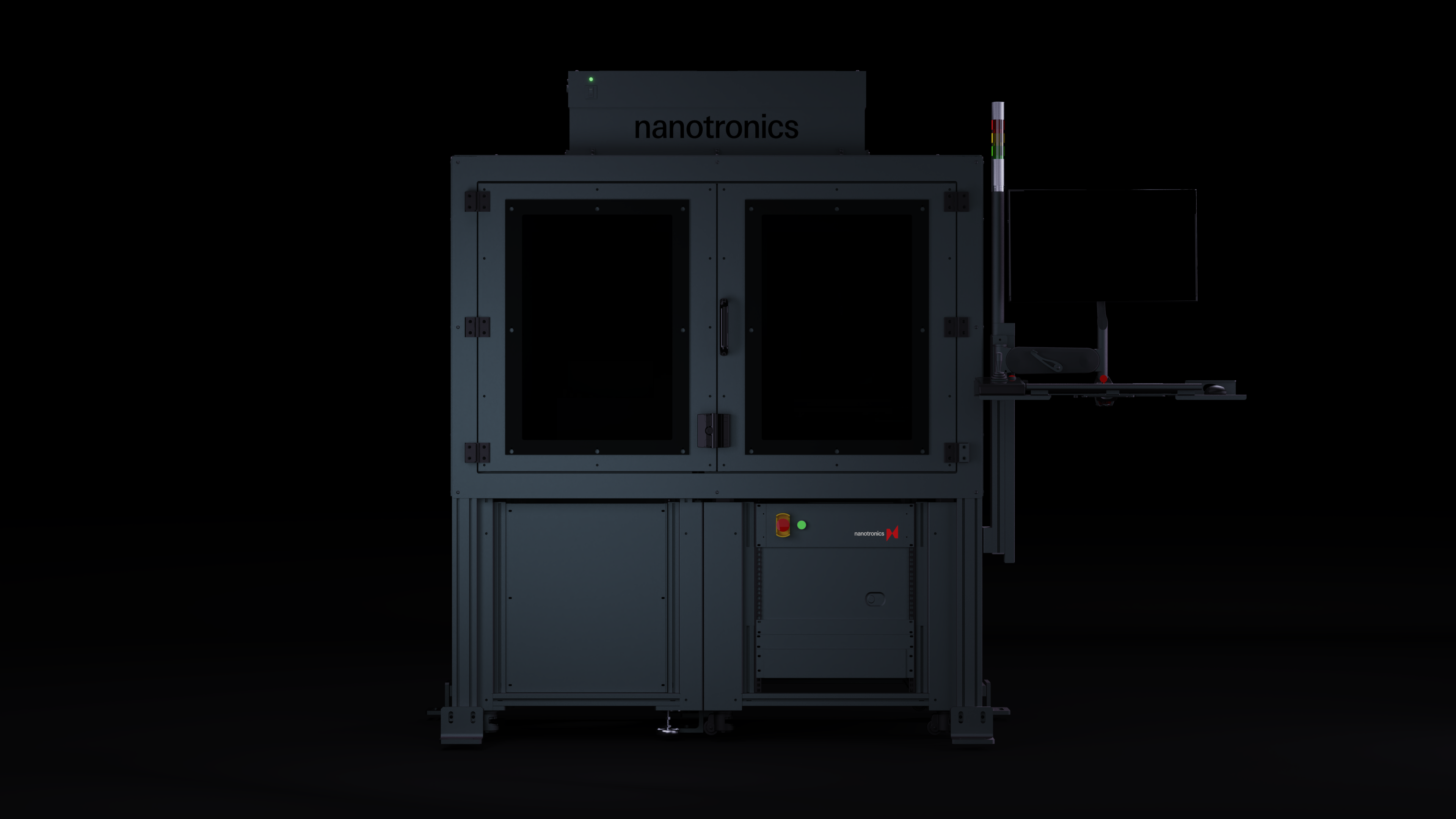
nSpecPRISM
The nSpec PRISM offers a complete solution for compound semiconductor front-end wafer production, from unpolished substrates to epitaxy and device manufacturing.
System highlights
Throughput Up to 6 wafers / hour
Max wafer size200mm
Scan resolution0.9 µm/ pixel (w/ 5x objective)

Benefits
Defect types
Soldering defects
Identify imperfections in soldering to prevent poor electrical connections and increase device reliability
Foreign material contamination
Identify small particles from equipment or the environment during processing
Industries
Our solutions are tailored to meet the unique challenges and demands of each sector.
Downloads
Contact Us